- 您现在的位置:买卖IC网 > Sheet目录1993 > DS1375T+ (Maxim Integrated Products)IC RTC SERIAL W/ALARM 6-TDFN
DS1375
I2C Digital Input RTC with Alarm
_____________________________________________________________________
7
month register) is toggled when the years register over-
flows from 99 to 00.
The day-of-week register increments at midnight.
Values that correspond to the day of week are user-
defined but must be sequential (i.e., if 1 equals
Sunday, then 2 equals Monday, and so on). Illogical
time and date entries result in undefined operation.
When reading or writing the time and date registers,
secondary (user) buffers are used to prevent errors
when the internal registers update. When reading the
time and date registers, the user buffers are synchro-
nized to the internal registers on any START or STOP
and when the register pointer rolls over to zero. The
time information is read from these secondary registers,
while the clock continues to run. This eliminates the
need to reread the registers in case the main registers
update during a read.
The countdown chain is reset whenever the seconds
register is written. Write transfers occur on the acknowl-
edge from the DS1375. Once the countdown chain is
reset, to avoid rollover issues the remaining time and
date registers must be written within 1 second. The 1Hz
square-wave output, if enabled, transitions high 500ms
after the seconds data transfer, provided the clock
input is already being driven.
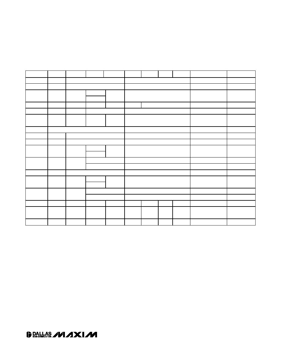
Table 1. Timekeeping Registers and SRAM
ADDRESS
BIT 7
BIT 6
BIT 5
BIT 4
BIT 3
BIT 2
BIT 1
BIT 0
FUNCTION
RANGE
00h
0
10 Seconds
Seconds
00–59
01h
0
10 Minutes
Minutes
00–59
AM/PM
02h
0
12/24
10 Hours
Hours
1–12 + AM/PM
00–23
03h
0
Day
1–7
04h
0
10 Date
Date
00–31
05h
Century
0
10
Month
Months
Month/
Century
01–12 +
Century
06h
10 Year
Year
00–99
07h
A1M1
10 Seconds
Seconds
Alarm 1 Seconds
00–59
08h
A1M2
10 Minutes
Minutes
Alarm 1 Minutes
00–59
AM/PM
09h
A1M3
12/24
10 Hours
Hours
Alarm 1 Hours
1–12 + AM/PM
00–23
Day
Alarm 1 Day
1–7
0Ah
A1M4
DY/DT
10 Date
Date
Alarm 1 Date
1–31
0Bh
A2M2
10 Minutes
Minutes
Alarm 2 Minutes
00–59
AM/PM
0Ch
A2M3
12/24
10 Hours
Hours
Alarm 2 Hours
1–12 + AM/PM
00–23
—
Day
Alarm 2 Day
1–7
0Dh
A2M4
DY/DT
10 Date
Date
Alarm 2 Date
1–31
0Eh
ECLK
CLKSEL1
CLKSEL0
RS2
RS1
INTCN
A2IE
A1IE
Control
—
0Fh
0
A2F
A1F
Control/
Status
—
10h–1Fh
B7
B6
B5
B4
B3
B2
B1
B0
SRAM
00–FFH
发布紧急采购,3分钟左右您将得到回复。
相关PDF资料
DS1384FP-12+
IC CTRLR RTC WDOG 120NS 44-MQFP
DS1386P-8-120+
IC TIMEKEEPER RAM 64K 34-PCM
DS1388Z-3+T&R
IC RTC I2C W/CHARGER 8-SOIC
DS1391U-3+
IC RTC W/CHARGER 10-USOP
DS1394U-33+T&R
IC RTC SPI 3WIRE W/CHRGR 10-MSOP
DS14285SN+T&R
IC RTC W/NV RAM CNTRL 24-SOIC
DS1486P-120+
IC TIMEKEEPER RAM 1MB 34-PCM
DS1500WE
IC RTC Y2KC W/NV CTRL 32-TSOP
相关代理商/技术参数
DS1375T+T&R
制造商:Maxim Integrated Products 功能描述:REAL TIME CLOCK SERL 6TDFN EP - Tape and Reel 制造商:Maxim Integrated Products 功能描述:IC RTC SERIAL W/ALARM 6TDFN
DS1375T+T&R
功能描述:实时时钟 I2C Digital Input w/Alarm RoHS:否 制造商:Microchip Technology 功能:Clock, Calendar. Alarm RTC 总线接口:I2C 日期格式:DW:DM:M:Y 时间格式:HH:MM:SS RTC 存储容量:64 B 电源电压-最大:5.5 V 电源电压-最小:1.8 V 最大工作温度:+ 85 C 最小工作温度: 安装风格:Through Hole 封装 / 箱体:PDIP-8 封装:Tube
DS1380N
制造商:未知厂家 制造商全称:未知厂家 功能描述:NVRAM (Battery Based)
DS1380S
制造商:未知厂家 制造商全称:未知厂家 功能描述:NVRAM (Battery Based)
DS1380SN
制造商:未知厂家 制造商全称:未知厂家 功能描述:NVRAM (Battery Based)
DS1384
制造商:DALLAS 制造商全称:Dallas Semiconductor 功能描述:Watchdog Timekeeping Controller
DS1384FP
制造商:MAXIM 制造商全称:Maxim Integrated Products 功能描述:Watchdog Timekeeping Controller
DS1384FP-12
功能描述:IC CTRLR RTC WDOG 120NS 44-MQFP RoHS:否 类别:集成电路 (IC) >> 时钟/计时 - 实时时钟 系列:- 产品培训模块:Obsolescence Mitigation Program 标准包装:1 系列:- 类型:时钟/日历 特点:警报器,闰年,SRAM 存储容量:- 时间格式:HH:MM:SS(12/24 小时) 数据格式:YY-MM-DD-dd 接口:SPI 电源电压:2 V ~ 5.5 V 电压 - 电源,电池:- 工作温度:-40°C ~ 85°C 安装类型:表面贴装 封装/外壳:8-WDFN 裸露焊盘 供应商设备封装:8-TDFN EP 包装:管件